Available Monday, June 20, 2001
Due Wednesday, July 4, 2001
Due by 3:30 pm on Wednesday, July 4, in the CMPT-150-ARC drop boxes outside K9507. Make sure you put your assignment in the box labeled for CMPT-150-ARC.
PLEASE NOTE: Part of this assignment must be submitted electronically!
Total: 40 marks
Question 1. ROMs are frequently used as lookup tables,
which store pre-computed values of functions. Consider the function
y = 3x + 2
What values will be stored in the ROM (and where) for x = {0..5}? What
size of memory is required?
SOLUTION (6 marks)
To choose the size of the ROM, we need two values - word length and
number of words. Since the words are addressed using binary encoding, the
number of words must be a power of two. There are 6 possible input values
for the ROM - x=0 to x=5, so we need 8 words (4 would be too few) and therefore
3 address lines.
The word size depends on how we store the data, and how big each piece
of data is. To discover this, we need the answer to the function for x=0
through x=5 (besides, that's part of the assignment!):
|
|
|
binary |
|
|
|
10 |
|
|
|
101 |
|
|
|
1000 |
|
|
|
1011 |
|
|
|
1110 |
|
|
|
10001 |
Since the biggest number to be stored in the ROM is 1710
(which is 100012), our ROM needs 5-bit words.
So the ROM will be 8x5, and the values stored in it will be as
follows:
|
|
|
|
|
|
|
|
|
|
|
|
|
|
|
|
|
|
|
|
|
|
|
|
|
|
|
It is unimportant (i.e. don't care) what values are stored for addresses 6 and 7, because the problem only asked us to store data for values 0..5.
Question 2. Sequential logic can be used to design things other than just counters. A door lock is to be designed given the following constraints.
SOLUTION (15 marks)
The first thing to do is decide how many states there will be in this
machine. There should be a default state to return to when an
incorrect button is pressed, and there should be a state for each progressive
correct button. Thus if the initial state is referred to as state
0, pressing button "A" will move the device to state 1, from there "B"
will move the device to state 2, another "B" will move the device to state
3. At this point we need to make a design decision. the final
"A" could move the device to a 5th state, or it could simply trigger the
door opening and return to the initial state. the 5th state would
require an extra flip-flop as well as extra input and output designs, so
we will avoid that. An incorrect button press from any state will
return the device to the initial state.
Our states are then as follows:
00 - no correct inputs
01 - "A" correct
10 - "AB" correct
11 - "ABB" correct
Since the buttons cannot be pressed together, AB=11 is a don't care condition.
If no button is pressed, we will stay in the same state, because we assume that the user is not as fast as the clock and mmust wait a while between button presses.
We will also assume that there is some hardware at the switches to turn a button press into a single pulse of "A" or "B", across the appropriate clock edge.
We will aslo assume that there is some hardware at the door lock to take a single pulse from the "Unlock" signal and hold the lock open until the door is used.
We have a transition table. amd corresponding D-FF truth table:
|
|
|
|
|
|
|
|
|
|
||
|
|
|
|
|
|
|
|
|
|
||
|
|
|
|
|
|
|
|
|
|
||
|
|
|
|
|
|
|
|
|
|
||
|
|
|
|
|
|
|
|
|
|
||
|
|
|
|
|
|
|
|
|
|
||
|
|
|
|
|
|
|
|
|
|
||
|
|
|
|
|
|
|
|
|
|
||
|
|
|
|
|
|
|
|
|
|
||
|
|
|
|
|
|
|
|
|
|
||
|
|
|
|
|
|
|
|
|
|
||
|
|
|
|
|
|
|
|
|
|
||
|
|
|
|
|
|
|
|
|
|
||
|
|
|
|
|
|
|
|
|
|
||
|
|
|
|
|
|
|
|
|
|
||
|
|
|
|
|
|
|
|
|
|
||
|
|
|
|
|
|
|
|
|
|
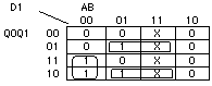
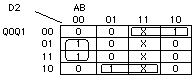
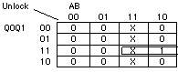
We must now do K-maps for D0, D1, and Unlock:
And the equations are:
D1=/Q0Q1B + /A/BQ0 + Q0/Q1B
D2=Q1/A/B + /Q0/Q1A + Q0/Q1B
Unlock = Q0Q1A
The circuit is like this:
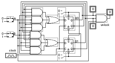
and the timing diagram:
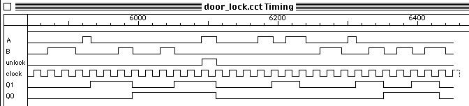
There are a few things to make note of on the diagram.
Question 3. Using the 5 instructions in the SAP-1 instruction
set, write an assembly language program which will present as output the
solution to the following expression:
1210 + 910 - 510
SOLUTION (8 marks)
Given the example program in the SAP-1 notes, we can model our new
program around that. We'll put our data at the end of memory using
labels, as in the example program: 1210 = 0C16,
910 = 0916, 510 = 0516.
op1: db 0cHThen, we can write the program assuming those variables. The result should be 1610 = 1016.
op2: db 09H
op3: db 05H
A4q3: lda op1 ;A <- 0cH
add op2 ;A <- A + 09H = 15H
sub op3 ;A <- A - 5H = 10H
out ; display result
hlt ; stop executionop1: db 0cH
op2: db 09H
op3: db 05H
Question 4. Given the complete hardware for the SAP-1
as given in class and in the on-line notes, you are to add sufficient hardware
to allow the SAP-1 to perform the operation "stpc". stpc
should store the contents of the program counter in the address specified
in the address field of the instruction. The opcode for stpc
should be 0011. Justify any design decisions. Describe the
operation of the new instruction, using english or the "register transfer"
notation discussed in class.
SOLUTION (8 marks)
We can start by examining what the new instruction needs to do, and
how we propose to do it. First, we see that the new instruction needs
to move the PC tp the memory. We can do this through the bus.
The hardware as it stands allows the PC to drive the bus, so we're ok there.
What we can't do is write to memory, so the task is to modify the memory
so that it can read from the bus:
The new hardware looks like this:
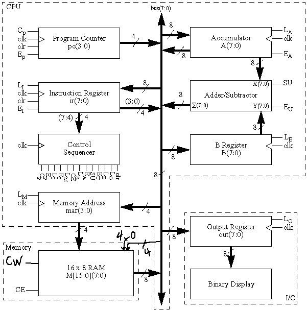
And the new instruction will operate as follows. Note that the
first 3 clock cycles are the standard fetch.
| Step | Action | Control Points | Description |
| T1 | mar <- pc | EP,LM | address of current instruction is placed in memory address register |
| T2 | pc <- pc+1 | CP | pc gets address of next instruction |
| T3 | ir <- M[mar] | CE,LI | the instruction is fetched from memory and placed into ir |
| T4 | mar <- ir(3:0) | EI,LM | address field of instruction is used to address the memory |
| T5 | M[mar](3:0) <- pc
M[mar](7:4) <- 0000 |
CW,EP | value in program counter is written to memory at the specified address. |
| T6 | noop | - | done, so wait for the 6th cycle to pass. |
Question 5. This question will verify that you are able to use the web-based electronic submission system. Generate a text document (using notepad, simpletext, or some other text editor) stating your name, student number and the date, and submit this file using the electronic submission system (use .zip format). You must let me know SOON if electronic submission is unreasonable for you. Remember that this can be done from on-campus computers.
SOLUTION: successful submission, 3 marks.
Further instructions follow:
CMPT Assignment Submission Web Service
provided by
School of Computing Science
at Simon Fraser University
--------------------------------------------------
Assignments Submission Web - For Registered CMPT Students Only
https://onara.cs.sfu.ca/
--------------------------------------------------
This service is meant to be used by students that are currently registered in Computing Science courses whose instructor has chosen to make use of this Submit Server. Students can submit their course assignments via Internet, from any computer. Please check with your course instructor to see if he/she plans to use this service for the course.
HOW TO USE THIS SERVICE:
You have to provide identification in a number of places, for security purposes. Please remember that you have to use your SFU account id. That password is initially set to your 9-digit student number and it can be changed through the GradeBook website. Once you have changed your password for the GradeBook, you should be able to use your new password here within 10 minutes. Occasionally, due to unexpected network problems, there may be a longer delay. If you need to submit your assignment right away, you should be able to use your old (unchanged) password.
You can submit only one file as an assignment. Files submitted must be either in zip or gzip format. Please check with your instructor for the preferred format for your course. The size limit on submitted files is 1M. You can submit your assignment up to thirty times, but only one copy is kept on the server: the latest submitted file. Assignments submitted after the deadline specified by the instructor are still accepted, but they are marked as late, with a timestamp. The instructor determines the policy on late assignments, and it is up to the student to learn the policy. Submission can take some time, and the server may become quite busy and slow near the deadline for assignments, especially in large classes. Give yourself some time to submit.
WARNING: If you submit a file in time but decide to re-submit after the deadline, the only copy kept is the LATE one!
If you have any questions, please address them by e-mail to csilop@cs.sfu.ca.
IMPORTANT! Please TEST your user id and password at
https://onara.cs.sfu.ca/submit/test/
as soon as you find out that you are going to use this service ( preferably
at least one week before the first assignment ). In case of any failure,
please report it as soon as possible to
csilop@sfu.ca.
NOTE: This application will work only if you are using Netscape Navigator
2.0 or newer or Internet Explorer 3.02 or newer. Internet Explorer prior
to version 3.02 cannot upload files. You have to add this capability with
the File Upload Add-On or you can upgrade to newer versions of Internet
Explorer.